
ライター:mpcsp079さん(最終更新日時:2016/5/21)投稿日:2014/11/18
.
LM2917の動作を調べた
■ことの起こり、質問
http://detail.chiebukuro.yahoo.co.jp/qa/question_detail/q14138277169
LM2917について、度々たびすいません!
少しですがデータシートの内容が理解できてきました。
(恥ずかしいところですが、freq=RPMと勘違いしていたので、理解するのに非常に時間をかけましたw)
http://www.ti.com/lit/ds/slfs011a/slfs011a.pdf
質問 A) 今までに質問していた回路では、比較的LEDゲージ向けなもので、精度を上げるには、基本的にC1を低め、R1を大きめに設計したほうが望ましいのですか?
質問 B) fmaxの許容する範囲で、Vrippleを減少させるためにC2のキャパシタの値を増やしても大丈夫でしょうか?
http://yahoo.jp/box/zliE5H
之で合っているのかわかりませんが、計算用のシートをCalcで作ってみました
http://detail.chiebukuro.yahoo.co.jp/qa/question_detail/q14138277169
ICデータシート
http://www.ti.com/lit/an/snaa088/snaa088.pdf#search='lm2907+chagepump'
http://www.ti.com/lit/ds/slfs011a/slfs011a.pdf
■LM2917の使い方
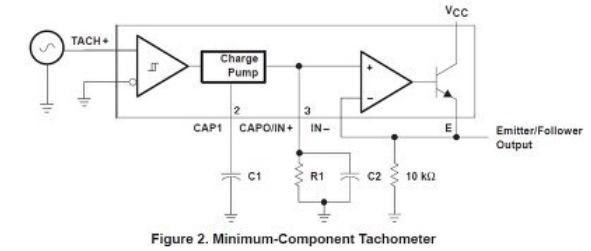
図1 LM2917の使用例
3pinの電圧VOは、
VO = VCC • f • C1 • R1 ---(a1)
これは下の解説で証明される。-->(6)式
Vripple =(VCC/2)(C1/C2)(1ー VCC* f* C1/200μA) --(a2)
• • • • ) volts peak-to-peak
データシートは間違いで、200-->200μA
下解説図6参照ず
図6で
2t=T
になったとき、リップルはなくなる。(1)式より
t=C1*V/I
I=200μA
V=Vcc/2
下の(1)式より、
2t=C1*(Vcc)/200μA
また、
T=1/f
よって、
C1*(Vcc)/200μA=1/f
のとき、リップルは=0となる。
これで、(a2)式がわかる。
ここから、2t=Tになる点でVOが頭打ちになることが、図6からわかる。
つまり、
1/Tmin=fmax =Icap/(C1 *VCC) hertz
where:
Icap is typically 200 μA,
C1 is in farads, and
VCC is in volts.
ここで、
http://www.ti.com/lit/ds/slfs011a/slfs011a.pdf
では、
Icap is typically 200 μAになっている。200μAが正しい。たのところでは、200、200mAとなっているが、間違いである。
これが、2t=Tとなる点で、これ以上の周波数は測れない。
■設計手順
fmax =Icap/(C1 *VCC)
からC1が決まる。C1の最大値C1maxは、
C1max=Icap/(fmax *VCC)
Icap=200μA
C1はこれ以下にする。
下の(1){式より、
2t =C1*Vcc/200μA
であるので、2tが大きいほどリップルは小さくなる。つまり、C1をC1maxにしたときにリップルは最小にできる。 C1=C1maxにすべきである。
さらに、
VO = VCC • f • C1 • R1
から、
f0の時のVOをVO0としたければ、
VO0 = VCC • f0 • C1 • R1
R1=VO0/( VCC • f0 • C1)
C2はVOの遅れ可能時間をTdとすれば、
R1*C2<Td
になるようにする。
リップルはこれで決まってしまう。低回転になるほどリップルは大きくなる。
■LM2917の詳細
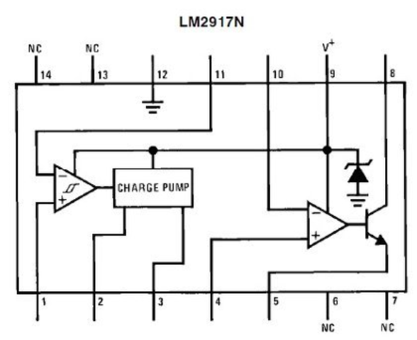
図2 LM2917ブロック図
全体回路を図3にしめす。

図3 LM2917全体回路
チャージポンプ部分を図4に示す。
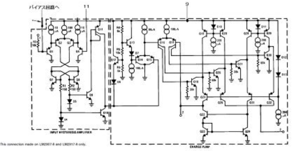
図4 LM2917、アンプ、チャージポンプ部分
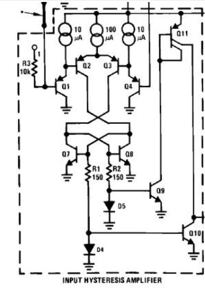
図5-1 ヒステリシスコンパレータ
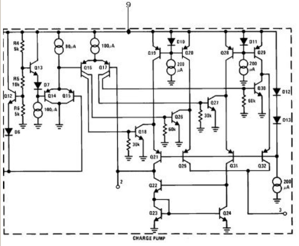
図5-2 チャージポンプ部
■解説 Input Hysteresis Amplifier
The equivalent schematic diagram is shown in Figure 2. Q1through Q11 comprise the input hysteresis amplifier. Q1through Q4 comprise an input differential amplifier which, byvirtue of PNP level shifting, enables the circuit to operate with signals referenced to ground. Q7, Q8, D4, and D5 comprise an active load with positive feedback. This load behaves as a bi-stable flip-flop which may be set or reset depending upon the currents supplied from Q2 and Q3. Consider the situation where Q2 and Q3 are conducting equally, i.e. the input differential voltage is zero. Assuming Q7 to be conducting, it will be noted that the current from Q3 will be drawn by Q7 and Q8 will be in the ``OFF'' state. This allows the current from Q2 to drive Q7 in parallel with D4 and a small resistor. D4 and Q7 are identical geometry devices, so that the resistor causes Q7 to be biased at a higher level than D4. Thus Q7 will be able to conduct more current than
Q3 provides. In order to reverse the state of Q7 and Q8, it will be necessary to reduce the current from Q2 below that provided by Q3 by an amount which is established by R1.
It can be shown that this requires a differential input to Q1 and Q4, of approximately 15mV. Since the circuit is symmetrical, the threshold voltage to reverse the state is 15 mV in the other direction. Thus the input amplifier has built-in hysteresis at g15 mV. This provides clean switching where noise may be present on the input signal, and allows total rejection of noise below this amplitude where there is no input signal.
■アンプ解説の訳
図4でQ1からQ11まではインプットヒステリシスアンプである。Q1からQ4までは差動アンプで、レベルシフトもしている。Q7,Q8,D4,D5は正の帰還による能動負荷である。この負荷は2安定のフリップフロップとなる。Q2,Q3からの電流によりセット、リセットされる。
Q2,Q3が同じ導通であるときを考える。ゆえにIN差動電圧は=0である。Q7が導通であるとすると、Q3からの電流はQ7に流れ、Q8はOFFになる。
これは、D4と小抵抗と並列なQ2からの電流がQ7をドライブすることを許す。抵抗がD4とQ7はD4より高いレベルでQ7がバイアスされるように、理想的寸法である。このためQ7はQ3より多くの電流を流すことができる。Q7,8の状態を反転させるために、R1とQ3によるQ2からの電流を減らすことが必要である。
Q1,Q4への差動インプットが15mVであることは示される。回路が対称であるから、反転させる閾値電圧は15mVである。それゆえ、インプットアンプは15mVのヒステリシスをもつ。このため、ノイズによるスイッチングを避けることができる
■解説Charge Pump
The charge pump is composed of Q12 through Q32. R4, R5,and R6 provide reference voltages equal to 1/4 and 3/4 of supply voltage to Q12 and Q13. When Q10 turns ``ON'' or ``OFF,'' the base voltage at Q16 changes by an amount
equal to the voltage across R5, that is 1/2 VCC. A capacitor connected
between Pin 2 and ground is either charged by Q21 or discharged by Q22
until its voltage matches that on the base of Q16. When the voltage on Q16
base goes low, Q16 turns ``ON,'' which results in Q18 and Q26 turning on,
which causes the current, sourced by Q19 and Q20, to be shunted to ground. TThus Q21 is unable to charge pin 2. Meanwhile, Q27 and Q30 are turned off
permitting the 200 mA sourced by Q28 and Q29 to enter the emitters of Q31 and Q32 respectively. The current from Q31 is mirrored by Q22 through Q24
resulting in a 200 mA discharge current through pin 2. The external capacitor on pin 2 is thus discharged at a constant rate until it reaches the new base
voltage on Q16. The time taken for this discharge to occur is given by:
t =C1*V/I --(1)
where C1 = capacitor on pin 2
V = change in voltage on Q16 base
I = current in Q22
During this time, Q32 sources an identical current into pin 3. A capacitor
connected to pin 3 will thus be charged by the same current for the same
amount of time as pin 2. When the base voltage on Q16 goes high, Q18 and Q26 are turned off while Q27 and Q30 are turned ``ON.'' In these conditions, Q21 and Q25 provide the currents to charge the capacitors on pins 2 and 3
respectively.
Thus the charge required to return the capacitor on pin 2 to the high level voltage is duplicated and used to charge the capacitor connected
to pin 3. Thus in one cycle of input the capacitor on pin 3 gets charged twice
with a charge of C1*V.
Thus the total charge pumped into the capacitor on pin 3 per cycle is:
Q = 2 C1*V -- (2)
Now, since V =VCC/2
then Q =C1*VCC -- (3)
A resistor connected between pin 3 and ground causes a discharge of the
capacitor on pin 3, where the total charge drained per cycle of input signal is
equal to:
Q1=V3 *T/R1
where V3 = the average voltage on pin 3
T = period of input signal
R1 = resistor connected to pin 3
In equilibrium Q = Q1
i.e., C*VCC =V3* T/R1 ーー(4)
and V3 = VCC *R1*C1/T -- (5)
or V3 =VCC * R1 * C1*f --(6)
where f e input frequency
■チャージポンプ部の訳
チャージポンプ回路はQ12からQ32で構成されている。R4,R5、R6はQ12,Q13に供給する電源電圧の1/4、3/4の電圧を作る。Q10がONかOFFに変化したとき、Q16のベース電圧はR5の電圧に等しい値により変化する。それはVcc/2である。2ピンとGND間につながれたキャパシタは、その電圧がQ16のベース電圧になるまで、Q21により充電され、Q22により放電される。.
Q16のベースが低くなったとき、Q16はONになる。そのため、Q18,Q26はONに変化する。これは、GNDに電流が逃がされるから、Q19,Q20により送られている電流を変える。このためQ21は2ピンを充電できない。他方、Q27,Q30はOFFされ、Q31,Q32のエミッタには、Q28,Q29の電流200mAが流される。このQ31からの電流は、Q24、Q22の電流ミラーにより2ピンの200mAの放電電流となる。2ピンにつながれたキャパシタは一定レートでQ16の新しいベース電圧に到達するまで放電していく。この時間は次になる。
t =C1*V/I --(1)
where C1 = capacitor on pin 2
V = change in voltage on Q16 base
I = current in Q22(=200μA)
この時間の間、Q32は3ピンへ電流を流しこむ。3ピンにつながれるキャパシタは2ピン同じ時間、同じ電流で充電される。Q16のベース電圧がハイになると、Q18,Q26は、Q27,Q30がONに変わる間、OFFに変わる。Q21,Q25は2,3ピンのキャパシタを充電する電流を作る。
2ピンのキャパシタをハイレベル電圧に戻すための電荷は複製され、3ピンにつながれたキャパシタを充電するのに使われる。インプットの1サイクルで3ピンのキャパシタはC*Vの電荷の2倍となる。3ピンのキャパシタに1サイクル当たり送られる全電荷は
Q = 2 C1*V -- (2)
Now, since V =VCC/2
then Q =C1*VCC -- (3)
3ピンとGND間につながれた抵抗(R1)は3ピンのキャパシタを放電させる。ここで1サイクルあたりの全放電電荷は、
Q1=V3 *T/R1
where
V3 =the average voltage on pin 3
T = period of input signal
R1 = resistor connected to pin 3
In equilibrium Q = Q1
i.e. , C1*VCC =V3* T/R1 ーー(4)
and V3 = VCC *R1*C1/T -- (5)
or V3 =VCC * R1 * C1 *f --(6)
where f e input frequency
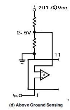
■Input Interface Circuits
The ground referenced input capability of the LM2907-8 allows
direct coupling to transformer inputs, or variable reluctance
pickups. Figure 5(a) illustrates this connection. In
many cases, the frequency signal must be obtained from
another circuit whose output may not go below ground. This
may be remedied by using ac coupling to the input of the
LM2907 as illustrated in Figure 5(b). This approach is very
suitable for use with phototransistors for optical pickups.
Noisy signal sources may be coupled as shown in Figure
5(c). The signal is bandpass filtered. This can be used, for
example, for tachometers operating from breakerpoints on a
conventional Kettering ignition system. Remember that the
minimum input signal required by the LM2907 is only 30
mVp-p, but this signal must be able to swing at least 15 mV
on either side of the inverting input. The maximum signal
which can be applied to the LM2907 input, is g28V. The
input bias current is a typically 100 nA. A path to ground
must be provided for this current through the source or by
other means as illustrated. With 14-pin package versions of
LM2907, LM2917, it is possible to bias the inverting input to
the tachometer as illustrated inFigure 5(d). This enables the
circuit to operate with input signals that do not go to ground,
but are referenced at higher voltages. Alternatively, this
method increases the noise immunity where large signal
levels are available but large noise signals on ground are
also present. To take full advantage of the common-mode
rejection of the input differential stage, a balanced bias configuration
must be provided. One such circuit is illustrated in
Figure 5(e). With this arrangement, the effective commonmode
rejection may be virtually infinite, owing to the input
hysteresis.
1ピンのIN信号は11ピンの電圧に対して最低±15mV振れなくてはいけない。信号がGND以上である場合は11ピンをGNDとVccの中間にしなくてはいけない。
■リップル
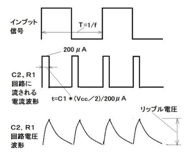
図6 リップル
図7のようにLM2917に入れる信号はデューティー比は50%でないとだめである。そうでないとCPOの出方が不均一になる。針状のパルスである場合、図8のようなことをやらなければいけない。
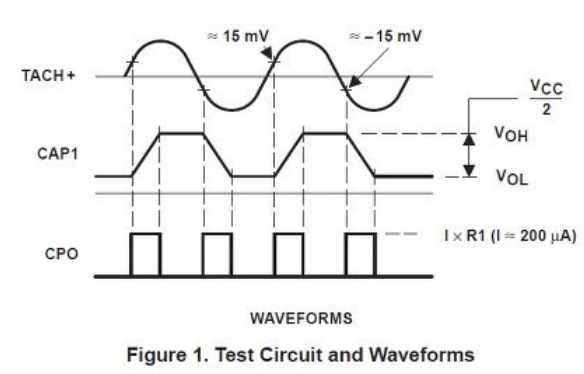
図7 LM2917の入れる波形はデューティー比は50%でないとだめ
図8 波形の変換