インバータ発振回路について

CMOSインバータと水晶(セラミック振動子)による発振器について考えてみた
コルピッツ発振器の原理 - SonofSamlawのブログ (hatenablog.com)
も参考に
CMOSインバータは図1のようになっている。

図1 CMOSインバータ
VOLは電流源である。ここが肝心で、電圧源ではいけない。だからTTLではいけないのである。
発振回路は図2である。

図2 発振器
図2を少し書き変える。
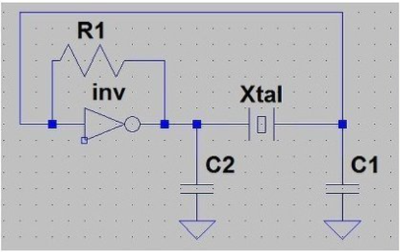
図3 図2の変形
R1はMOSトランジスタのゲートにバイアス電流を供給し、かつバイアス点を確立するためにある。しかし、これによりゲインが制限されてしまうので、高い周波数でやる場合は、これをなくすことにする。このとき、バイアス電流やバイアス点はどうなってしまうのかは不明である。これは大きい抵抗なので省略して考えてもよいので、図4に簡略化する。

図4 図3 の簡略化
インバータを図1で考え、さらに等価回路にすれば図5のようになる。

図5 図4の等価回路
図5はxtalをLに置き換えればコルピッツ発振器である。発振条件はvinからvoutまでの伝達周波数特性で、位相差0の周波数で、ゲイン>1 である。今、水晶発振子のモデルである図6を考える。Lに直列にC、それらに並列にCPが入ったとすれば(Rは無視)、
「コルピッツ発振回路の発振メカニズム」
コルピッツ発振器の原理 - SonofSamlawのブログ (hatenablog.com)
上記URL先記載の(6)(7)式のC1//C2をC12と書き、C3をCP、C4をC、L1をLとすれば、発振角周波数ω0は、
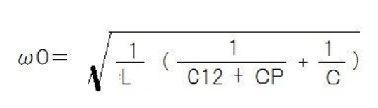
となる。
C12>>CP、C
とすれば、

となり、C1、C2には依存しなくなる。
資料1
http://www.eetasia.com/ARTICLES/2001SEP/2001SEP06_AMD_AN.PDF?SOURCES=DOWNLOAD
In this application note we shall discuss our recommended crystal oscillator circuit, explain each component in the circuit
and provide some guidelines on selecting values for these components. Finally, we shall give a few precautions to take in
order to avoid in-stability and start-up problems.

図6 xtalの等価回路(Fig.1)

図7 xtalのインピーダンス(Fig.2)
Figure 1. shows the crystal equivalent circuit. R is the effective series resistance, L and C are the motional inductance and capacitance of the crystal. CP is the shunt capacitance due to the crystal electrodes. Figure 2. shows the reactancefrequency plot of the crystal. When a crystal is operating at series resonance it looks purely resistive and the reactances of the inductor and the capacitor are equal (XL = XC). The series resonance frequency is given by the equation
fs=1/(2π√(LC))
When the crystal is operating in parallel resonant mode it looks inductive. The frequency of operation in this mode is defined by the load on the crystal. The crystal manufacturer should specify the load capacitance CL for parallel resonant crystals. In this mode the frequency of oscillation is given by the equation.
fa=1/(2π√(L(CLCP/(CL+CP))
In parallel resonance mode the crystal can be made to oscillate anywhere on the fs - fa slope of the reactance plot, shown in Figure 2, by varying the load of the crystal. All of MX-COM’s crystal oscillator circuits recommend using parallelresonant mode crystals.
Figure 3. shows the recommended Crystal oscillator circuit diagram. In this type of setup the crystal is expected to oscillate in parallel resonant mode. The inverter which is internal to the chip acts as class AB amplifier and provides approximately 180° phase shift from input to the output and the p network formed by the crystal, R1, C1 and C2 provides additional 180° phase shift. So the total phase shift around the loop is 360°. This satisfies one of the conditions required to sustain oscillation. The other condition, for proper startup and sustaining oscillation is the closed loop gain should be ³1.
The resistor Rf around the inverter provides negative feedback and sets the bias point of the inverter near mid-supply operating the inverter in the high gain linear region. The value of this resistor is high, usually in the range of a 500KW ~ 2MW. Some of MXCOM’s ICs have this resistor internal, refer to the external component specifications in the data sheet of a particular chip.

図8 発振回路
The capacitors C1 and C2 form the load capacitance for the crystal. The optimum load capacitance (CL) for a given crystal is specified by the crystal manufacturer. The equation to calculate the values of C1 and C2 is
CL=C1*C2/(C1+C2)+Cs
Where CS is the stray capacitance on the printed circuit board, typically a value of 5pf can be used for calculation purposes. Now C1 and C2 can be selected to satisfy the above equation. Usually C1 and C2 are selected such that they are approximately equal. Large values of C1 and/or C2 increases frequency stability but decreases loop gain and may
cause start-up problems.
R1 is the drive limiting resistor, the primary function of this resistor is to limit the output of the inverter so that the crystal is not over driven. R1 and C1 form a voltage dividing circuit, the values of these components are chosen in such a way that the output of the inverter goes close to rail-to-rail and the input to the crystal is 60% of rail-to-rail, usual practice is to make resistance of R1 and reactance of C1 equal at the operating frequency, i.e. R1 » XC1. This makes the input to the crystal half that of the inverter output. Always make sure that the power dissipated by the crystal is with-in the crystal manufacturer’s specifications. Over-driving the crystal may damage the crystal. Please refer to the crystal manufacturer’s recommendations.
Ideally the inverter provides 180° phase shift, but the inherent delay of the inverter provides additional phase shift proportional to the delay. In order to ensure the total phase shift of n360° around the loop, the p network should provide 180° less the phase shift due to the inverter delay. R1 can be varied to accomplish this. With fixed C1 and C2, the closed loop gain and phase can be altered by varying R1. In some applications R1 can be ignored if the above two conditions are met.
Some ICs have all the external components (Rf, R1, C1, and C2) internal to the chip, thus eliminating worries to the circuit designer. In this case simply connect the crystal across the XTAL and XTAL pins.
Hints:
Select a crystal with low effective series resistance (ESR), which helps with crystal start-up problems. Lower ESR increases the loop gain.
Reduce the stray capacitance on the board layout by shortening the traces. This would help with startup problem and as well as the frequency of oscillation.
Always test the circuit in applicable temperature and voltage ranges to ensure the crystal starts and sustains oscillations and tweak the component values if necessary.
For best results, a crystal oscillator design should drive the clock inverter input with signal levels of at least 40% of Vdd,peak to peak. Tuning fork crystals generally cannot meet this requirement. To obtain further crystal oscillator design assistance, consult your crystal manufacturer.
The recommended way to optimize R1 is first calculate C1 and C2 as explained earlier and connect a potentiometer in place of R1, set its initial setting at approximately equal to XC1, then vary the potentiometer setting if required until the crystal starts under all conditions and sustains oscillation under steady state condition.
資料2
http://eetimes.jp/ee/articles/1104/18/news092_2.html
日本語のもので、詳しく書いてあります。
資料3
水晶メーカー資料
http://www.ndk.com/jp/products/app/cu_001.html