サブレンジングAD変換入門 その1

Subranging, Error Corrected,
and Pipelined ADCs
Microsoft Word - Chapter 3 Data Converter Architectures F.doc (analog.com)
の
Subranging, Error Corrected, and Pipelined ADCsの部分のかなりおおざっぱ翻訳である。P3-61~P3-77
DA,AD変換解説 - SonofSamlawのブログ (hatenablog.com)
の3を参照
まだかきかけです。進めてまいります。
Because of the sheer complexity of constructing an all-parallel flash converter using
either vacuum tubes, transistors, or tunnel diodes, the early work such as in the Staffin
and Lohman 1956 (filed) patent in Reference 9 used subranging to simplify the
conversion process. However, in order to make the subranging ADC practical, a suitable
fast sample-and-hold was required. Early subranging ADCs using vacuum tube
technology were limited by the sample-and-hold performance, but by 1964 transistors
were widely available and Gray and Kitsopoulos of Bell Labs describe pioneering work
on the classic diode-bridge sample-and-hold in their 1964 paper (Reference 28).
A basic two-stage N-bit subranging ADC is shown in Figure 3.65. The ADC is based on
two separate conversions—a coarse conversion (N1 bits) in the MSB sub-ADC (SADC)
followed by a fine conversion (N2 bits) in the LSB sub-ADC. Early subranging ADCs
nearly always used flash converters as building blocks, but a number of recent ADCs
utilize other architectures for the individual ADCs.
【以上翻訳】
上位N1ビットと下位N2ビットに分けAD変換するのだ。それぞれのサブレンジADはFlash型を使う。2ステージNビットサブレンジングADCを図3.65に示す。上位レンジで変換値(DA変換でアナログに変換)とINアナログ値の差(誤差値)を下位レンジでAD変換する。

The conversion process begins placing the sample-and-hold in the hold mode followed by
a coarse N1-bit sub-ADC (SADC) conversion of the MSBs. The digital outputs of the
MSB converter drive an N1-bit sub-DAC (SDAC) which generates a coarsely quantized
version of the analog input signal. The N1-bit SDAC output is subtracted from the held
analog signal, amplified, and applied to the N2-bit LSB SADC. The amplifier provides
gain, G, sufficient to make the "residue" signal exactly fill the input range of the N2
SADC. The output data from the N1 SADC and the N2 SADC are latched into the output
registers yielding the N-bit digital output code, where N = N1 + N2.
【以上翻訳】
まずsub-ADCでN1ビットの変換する。そしてそれはsub-DACにも行く。これとアナログINが差し引かれ、その誤差値は増幅され、N2ビットLSBSADCにいく。増幅器はゲインGをもつ。それは、N2SADCのinput rangeを満たすようにするためである。N1,N2はNビットのデジタルデータとなる。
In order for this simple subranging architecture to work satisfactorily, both the N1 SADC
and SDAC (although they only have N1 bits of resolution) must be better than N-bits
accurate. The residue signal offset and gain must be adjusted such that it precisely fills
the range of the N2 SADC as shown in Figure 3.66A. If the residue signal drifts by more
than 1 LSB (referenced to the N2 SADC), then there will be missing codes as shown in
Figure 3.66B where the residue signal enters the out-of-range regions labeled "X" and
"Y". Any nonlinearity or drift in the N1 SADC will also cause missing codes if it exceeds
1 LSB referenced to N-bits. In practice, an 8-bit subranging ADC with N1 = 4 bits and
N2 = 4 bits represents a realistic limit to this architecture in order to maintain no missing
codes over a reasonable operating temperature range.
【以上翻訳】
十分な性能をだすためには、N1 SADCとSDACはN-bit精度よりよくなければならない。誤差値のおオフセットとゲインは、Fig.3.66Aに示すように、N2 SADCのレンジに合わせなければならない。もし誤差値がN2 SADCでの1LSBより大きく動いたなら、図3.66Bに示すような誤差波形となる。・・・
When the interstage alignment is not correct, missing codes will appear in the overall
ADC transfer function as shown in Figure 3.67. If the residue signal goes into positive
overrange (the "X" region), the output first "sticks" on a code and then "jumps" over a
region leaving missing codes. The reverse occurs if the residue signal is negative
overrange.
【以上翻訳】
あるステージの整合が修正されないとき、誤差は図3.67に示すようにADC全体の伝達特性に現れてしまう。
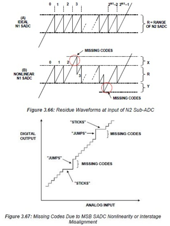
Figure 3.68 shows a popular 8-bit 15-MSPS subranging ADC manufactured by Computer
Labs, Inc. in the mid-1970s. This converter was a basic two-stage subranging ADC with
two 4-bit flash converters—each composed of 8 dual AM687 high speed comparators.
The interstage offset adjustment potentiometer allowed the transfer function to be
optimized in the field. This ADC was popular in early digital video products such as
frame stores and time base correctors.
【以上翻訳】
略す

In order to reliably achieve higher than 8-bit resolution using the subranging approach, a
technique generally referred to as digital corrected subranging, digital error correction,
overlap bits, redundant bits, etc. is utilized. This method was referred to in literature as
early as 1964 by T. C. Verster (Reference 29) and quickly became widely known and
utilized (References 30-33). The fundamental concept is illustrated in Figure 3.69.
【以上訳】
サブレンジ方式で8bit以上を実現するために、デジタル訂正サブレンジング、デジタル誤り訂正、オーバーラップビット、付加ビットなどのテクニックが使用される。この理論は1964年に論文になっている。図3,69に概要を示す。

A residue waveform is shown for the specific case where N1 = 3 bits. In a standard
subranging ADC, the residue waveform must exactly fill the input range of the N2
SADC—it must stay within the region designated R. The missing code problem is solved
by adding extra quantization levels in the positive overrange region X and the negative
overrange region Y. These additional levels require additional comparators in the basic
N2 flash SADC. The scheme works as follows. As soon as the residue enters the X
region, the N2 SADC should return to all-zeros and start counting up again. In addition,
the code 001 is added to the output of the N1 SADC to make the MSBs read the correct
code. The figure labels the uncorrected MSB regions on the lower part of the waveform
and the corrected MSB regions on the upper part of the waveform. A similar situation
occurs when the residue waveform enters the negative overrange region Y. Here, the first
quantization level in the Y region should generate the all-ones code, and the additional
overrange comparators should cause the count to decrease. In the Y region, the code 001
must be subtracted from the MSBs to produce the corrected MSB code. It is key to
understand that in order for this correction method to work properly, the N1 SDAC must
be more accurate than the total resolution of the ADC. Nonlinearity or gain errors in the
N1 SDAC affect the amplitude of the vertical portions of the residue waveform and
therefore can produce missing codes in the output.
【以上訳】
誤差値の波形はN1=3bitのときを示す。この誤差値はN1のINレンジを満たさなくてはいけない。それはRで示した領域に入らねばならない。誤変換問題は正のオーバー領域Xと負のオーバー領域で特別な量子化レベルを加えることで解決される。これらの付加されたレベルは、基本N2 flash SADCに付加されたコンパレータを必要とする。誤差がX領域に入るや否やN2 SADCはオールゼロにする。そして変換開始となる。001がMSBに訂正値を読ませるためにN1 SADCのOUTPUTに加えられる。図では波形の下の部分での未訂正MSB領域と、波形の上の部分での訂正MSB領域を区別している。似たような状況は誤差値波形が負のオーバーレンジ領域Yに入ったときにも起こる。ここで、Y領域での初めの量子化レベルは1だけのコードを発生させる。そして付加されたオーバーレンジコンパレーターはカウント値減少を引き起こす。Y領域で、001は訂正されたMSBを生み出すためにMSBから引かれなければならない。これらの訂正が確実な仕事となるためには、N1 SDACがADCの全体精度よりよい精度でなければならないことを理解することがカギとなる。N1 SDACの非線形やゲイン誤差は、誤差値波形の垂直成分の振幅に影響する。そのため、コード誤差の原因となる。
Horna in a 1972 paper (Reference 32) describes an experimental 8-bit 15-MSPS error
corrected subranging ADC using Motorola MC1650 dual ECL comparators as the flash
converter building blocks. Horna adds additional comparators in the second flash
converter and describes this procedure in more detail. He points out that the correction
logic can be greatly simplified by adding an appropriate offset to the residue waveform so
that there is never a negative overrange condition. This eliminates the need for the
subtraction function—only an adder is required. The MSBs are either passed through
unmodified, or 1 LSB (relative to the N1 SADC) is added to them, depending on whether
the residue signal is in range or overrange.
【以上訳】
Horna in は1972にモトローラMC1650のECLコンパレータにより、flashコンバータを構成し、実験的8bit 15-MSPSの誤差訂正サブレンジングADCを発表した。Hornaは第2flashコンバータに付加されたコンパレータを加え、この手順を詳細に説明している。彼は、消して負のオーバーレンジは生じないように誤差値波形にオフセットを加えることで論理回路を簡単にできることを指摘している。
MSBsはN1 SADCにおける1 LSBの付加か通過のみになる。
その2へ
サブレンジング(パイプライン)AD変換入門 その2 - SonofSamlawのブログ (hatenablog.com)