Hubert Houtman
4298 Masterson Rd., Blaine, WA 98230
September 18, 2000 • ELECTRONIC DESIGNから引用

T his sequential-sampling oscilloscope plug-in module can significantly increase the display bandwidth of an ordinary 10-MHz oscilloscope for repetitive signals (Fig. 1).
Using the 5k potentiometer and oscilloscope adjustments, the time base is
adjustable from 1 to 50 ns/div. For
longer sweeps, the circuit should simply be bypassed, and the oscilloscope
must be used directly. By adding a DSO
board and computer, it can be converted into a digital sampling oscilloscope as well. Future modifications,
such as the use of the strobe as a variable delay generator, are simple to put
into effect. Also easily implemented is
the “synchroscope” mode, with triggerable components installed within the
delay line.
The input signal enters via the compensator box, which is a 4.6-dB polezero cancellation attenuator.1 In
essence, the 40-pF capacitor diverts fast
changes into the 40-ns RG58A/U delay
line and away from the inductor arm.
As was verified by using this sampler as
a time-domain reflectometer (TDR),
the two main ports are 50 Ω up to 1
GHz. Frequency-dependent losses in
the delay cable are quite accurately
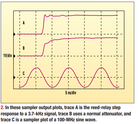
compensated, as shown by the reed-relay (Radio Shack part number 275-
232) step response (Fig. 2, trace A).
When an ordinary 4.6-dB attenuator is
implemented, a rounded step response
results (Fig. 2, trace B).
Although the inductor arm derives
the trigger from the input signal, other
triggers can be plugged in as needed.
These triggers also can be displayed by
routing them to the sampler via the delay line. For each input pulse, the
MAX961 trigger-and-hold comparator
triggers an adjustable-rate, fast-ramp
circuit by switching the two Schottkyclamped MPS-H10 transistors. At the
same time, its 4-V complementary-out
put step quickly enables its own latch
(LE), locking out further changes. This
locked comparator allows the switched
MPS-H81 current source to ramp up the
82-pF capacitor from −2 to 2 V, without
interruption. After 500 ns, the resistor
discharges the 1-nF capacitor to 0 V,
thereby reinstating the comparator and
re-arming the ramp.
The plus input of the MAX961 strobe
comparator is scanned by either a slow
ramp from the oscilloscope time-base
output (T), or the 250-Ω manual control (X) for the X-Y plotter. It’s scanned
over the same voltage range of −2 to 2 V,
which also is used as the display horizontal signal. Each time the fast ramp
crosses this voltage, the comparator
output switches from 2 to −2 V. Meanwhile, its complementary output
switches from −2 to 2 V. Both outputs
maintain a specified transition duration of 2.3 ns. They also symmetrically
drive the master/slave track-and-hold
bridges that are connected to sequentially sample VIN in
the delay cable.
The actual sampling event happens
in the track-to-hold
transition. It takes
place during the few
hundred picoseconds in which the
master Schottkydiode bridge resistance switches from
low to high. Such
switching occurs
within a small, central part of the full 8-
V applied step.
Consequently, its
switching duration
must be only a small fraction of the
strobe comparator transition duration.
The RC delay network controls the
strobe comparator’s latch. While the
slave is in the track mode, this latch
locks the master T/H in the hold state
for 650 ns.
During this 650-ns period, the master BIFET charge amplifier (1/2TL082)
can buffer the sample, pulsed onto its
input capacitance of about 15 pF. This
voltage is a scaled-down replica of the
sampled voltage entering the 1-pF/15-
pF capacitive divider. A 15M_/1M_ resistive divider is connected across it,
which completes this wideband compensated attenuator. Therefore, the
master bridge is loaded with only a
low-input capacitance of about 1 pF.
Because the bridge’s on-resistance is
about 100 Ω, the RC time constant is
around 100 ps.
Continuously buffering the 1-nF
memory, the slave T/H BIFET amplifier
(1/2TL082) produces a step-like, downconverted representation of the input
waveform (VIN). It does so at a low intermediate frequency (IF) for the oscilloscope, or a zero IF for the X-Y plotter.
Switching transients are eliminated via
the adjustable low-pass filter (LPF). By
averaging the output over as many input pulses as desired, this device
strongly reduces noise.
The bandwidth of this sampler is
over 1 GHz. Its transition duration is
about 300 ps which, together with the
approximately 250-ps intrinsic risetime
of the reed relay, yields the measured
display transition duration of 400 ps
(Fig. 2, trace A, again). Trace C illustrates the time-scale calibration and ver
-scale linearity by showing a sampled 100-MHz sine wave with a sampled zero line. For this RF measurement, a countdown trigger was used,
prior to the trigger-and-hold.2 To display higher frequencies with this sampler, the countdown trigger should be
preceded by a prescaler, such as the
emitter-coupled logic (ECL) circuitry.3
Additional experiments have verified
that it’s fairly easy to add more synchronized channels, using the strobe comparator to fan out and drive two or
more similar comparators. Via separate
delay lines, each of these comparators
drives individual T/H circuits to sample
multiple inputs.
References:
1. G. Amsel, R. Bosshard, R. Rausch,
and C. Zajde, “Time Domain Compensation Of Cable Induced Distortions
Using Passive Filters For The Transmission Of Fast Pulses,” Review of Scientific
Instruments, Vol. 42, No. 8, p. 1237-
1246, August 1971.
2. H. Houtman, “Counter Circuit Improves Oscilloscope Triggering,” Electronic Design, Vol. 48, No. 15, p. 126,
July 2000.
3. F.J. Hufft, “Build This 1.6-GHz
Counter Prescaler,” Radio-Electronics,
Vol. 61, 10, p. 47-54, October 1990.